

![]()
![]()
![]()
![]()
Nanoscale Metal Patterning of UHV Clean Semiconductor Surfaces
 |
 |
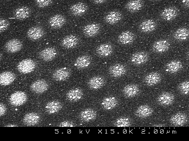 |
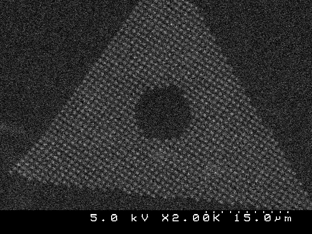
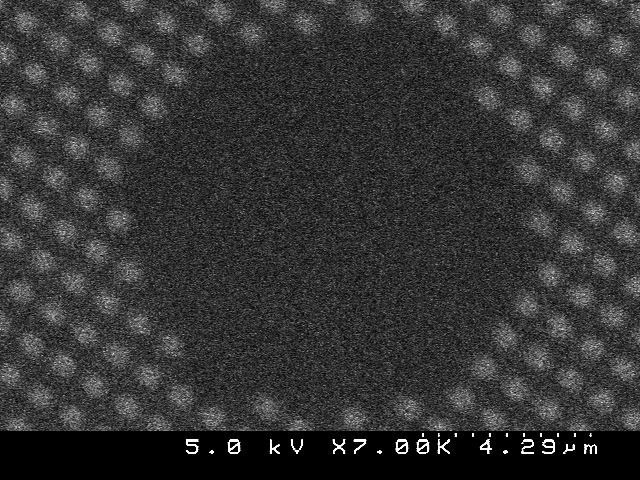
This work is focused on a process to create nanoscale features on a silicon substrate in ultra-high vacuum (UHV) using a silicon nitride nanostencil. The nanostencil, or shadow mask, consists of a 100nm thick silicon nitride membrane supported by a standard silicon wafer. Patterns of precisely aligned holes, of various sizes and shapes, were generated using the focused ion beam facility at UWO. The deposition process involves contact alignment of the nanostencil to the substrate, followed by metal evaporation. Analysis of the deposited patterns and nanostencil condition, post deposition, was carried out using scanning electron microscopy. Scanning tunneling microscopy (STM) was used to measure the metal coverage gradient created by the edge of the nanostencil. Feature edge definition of better than 200 nm has been achieved, implying a mask to sample spacing of less than 20 microns, even with simple optical alignment of the stencil to the substrate. Diffusion of the deposited metals has been observed by STM. This diffusion may place a limit on the ultimate resolution attainable by this method.
This work is supported by ![]()
Related Articles
A. Linklater and J. Nogami, “Defining nanoscale metal features on an atomically clean silicon surface with a stencil”
Nanotechnology, 19, 285302 (2008)
Ron Linklater's poster presented at NanoForum 2007 regarding nanostenciling. “Nanoscale Patterning of UHV Clean Si(001)”
R. Linklater and J. Nogami, University of Toronto ![]() .
.